


Technology
Multilayer PCBs
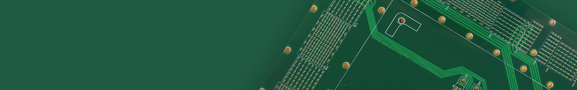
Your reliable PCB solutions provider
Due to the advent of the multi-layer printed circuit board industry, the number of these types of boards has increased significantly. They are commonly used in various electronic devices, such as Power Control systems, Servers, Electric Vehicles, Medical devices and 5G Base stations. JOVEPCB Enterprise Ltd. can produce these boards in various numbers, from small batches to large mass production. The maximum number of layers that the company can produce is 34 L.
JOVEPCB Enterprise Ltd. is a leading provider of printed circuit board manufacturing. We offer a wide range of solutions to our customers, which are some of the most innovative and exciting companies in the world. In conventional PCBs, we deliver exceptional quality and competitive prices. Through our global presence and advanced manufacturing capability, we are able to provide our customers with the peace of mind that they need.
Unlike other types of printed circuit boards, which are typically single-layer constructions, conventional multi-layer PCBs can be any number of layers with advanced technical requirements. Through our extensive capabilities, we are able to provide our customers with a complete solution that supports their various requirements at different design & NPI stages. Our PCB experts allow us to remain in step with the industry's technological demands.

What can we do?
For over two decades,JOVEPCB Enterprise Ltd. has been working on the production of power PCBs. It is capable of producing heavy copper boards with a thickness of up to 12oz. It is also proficient in various production processes such as metal half hole(castellation), buried blind hole, and resin plug hole.
JOVEPCB Enterprise Ltd. is a leading manufacturer of flat transformers, which are used for fast charging devices such as smartphones, tablets, and computers. Through its extensive production capacity and processing technology, it has been able to provide high-quality & reliability products and services to its customers.
Technical Characteristics
|
|
Manufacturing Process

AOI Test

Outer Layer Horizontal Line

Flying Probe Test

Laser Routing

Drilling Machine

Drilling Process

Auto Loading

Fixture of E-test

LDI

Drilling

AOI
Technical Parameter
| No. | Capabilities | Standard Production | Advanced Production | ||
|---|---|---|---|---|---|
| 1 | Panel size | Double sided | HASL | 544*800mm | 620*800mm |
| ENIG/Immersion Tin | 544*800mm | 620*1200mm | |||
| ≥4 layers | HASL | 544*650mm | 620*710mm | ||
| ENIG/Immersion Tin | 544*650mm | 620*710mm | |||
| 2 | Stack up | Blind/Buried board | Lamination times | MAX≤3times | MAX≤4times |
| Copper thickness | Inner layer | 1/2Oz-6Oz | 1/2Oz-12Oz | ||
| Outer layer | 1/2Oz-6Oz | 1/2Oz-12Oz | |||
| Min Dielectric ThK | 0.1mm | 0.043mm(≤3Oz) | |||
| Max Layer count | 24L | 34L | |||
| Final board ThK Tolerance | ThK≤1.0mm | ±0.1mm | ±0.1mm | ||
| ThK>1.0mm | ±10% | ±8% | |||
| 3 | Line/Space | Inner Layer | 1/2OZ | 4/4mil | 3/3mil |
| 1OZ | 5/5mil | 4/4mil | |||
| 2OZ | 7/7mil | 6/6mil | |||
| 3OZ | 8/8mil | 7/7mil | |||
| 4OZ | 10/10mil | 8/8mil | |||
| 5OZ | 12/12mil | 10/10mil | |||
| 6OZ | 14/14mil | 12/12mil | |||
| Outer layer | 1/3OZ | 4/4mil | 3/3mil | ||
| 1/2OZ | 4/4mil | 4/4mil | |||
| 1OZ | 5/5mil | 4.5/4.5mil | |||
| 2OZ | 8/8mil | 7/7mil | |||
| 3OZ | 10/10mil | 8/8mil | |||
| 4OZ | 12/12mil | 10/10mil | |||
| 5OZ | 14/14mil | 12/12mil | |||
| 6OZ | 16/16mil | 14/14mil | |||
| Pad Tolerance | ≤12mil | ±1.2mil | ±1.2mil | ||
| >12mil | ±10% | ±10% | |||
| 4 | Drill | Mechanical Drill size | 0.2-6.35mm | 0.1-6.35mm | |
| PTH Hole Tolerance | ±0.075mm | ±0.075mm | |||
| NPTH Hole Tolerance | ±0.05mm | ±0.05mm | |||
| Plated slot tolerance | Long slot | ±0.075mm | ±0.075mm | ||
| Short Slot | ±0.1mm | ±0.1mm | |||
| Aspect Ratio | DHS=0.15mm | 16:1 | 18:1 | ||
| DHS=0.2mm | 18:1 | 20:1 | |||
| DHS ≥0.25mm | 20:1 | 25:1 | |||
| Back drill(Back drill/Depth-control drill) | Hole size | 0.4-1.0mm | 0.4-6.35mm | ||
| Back drill relative to through hole | D+0.2mm | D+0.15mm | |||
| Back drill depth tolerance | ±0.1mm | ±0.08mm | |||
| Stub length | 0.05-0.25mm | 0.05-0.2mm | |||
| minimum distance between holes(different net) | 0.4mm | 0.3mm | |||
| minimum distance between holes(same net) | 0.25mm | 0.2mm | |||
| 5 | Min BGA | 1.0mm BGA 2 trace | Yes | Yes | |
| 0.8mm BGA 1 trace | Yes | Yes | |||
| 0.65mm BGA | Yes | Yes | |||
| 0.5mm BGA | Yes | Yes | |||
| 0.4mm BGA | Yes | Yes | |||
| 0.35mm BGA | No | Yes | |||
| 6 | Laser | Laser hole size | 0.075-0.2mm | 0.05-0.25mm | |
| Min. distance from laser hole to laser hole | 8mil | 5.5mil | |||
| Laser hole size | ≤0.8:1 | ≤1:1 | |||
| 7 | Soldermask | Color | Green,Yellow,Black,Blue,Red, White, Matt green | Green,Yellow,Black,Blue,Red, White, Matt green | |
| SM ThK | Single print thickness | 10-30um | 10-30um | ||
| Double print thickness | 20-60um | 20-60um | |||
| Trace knee | ≥5um | ≥5um | |||
| Min SM dam | normal color 4.0mil,other color min 5mil | normal color 3.0mil,other color min 4mil | |||
| 8 | Resin plugging | hole size | 0.15-0.6mm | 0.1-0.8mm | |
| PCB ThK | 0.5-4.5mm | 0.3-5.0mm | |||
| Resin plugging aspect ratio | 20:1 | 30:1 | |||
| 9 | Impedance | Capability of Impedance | Single line impedance<50Ω | ±5Ω | ±3.5Ω |
| Single line impedance≥50Ω | ±10% | ±7% | |||
| Differential line impedance | ±10% | ±7% | |||
| 10 | Testing Capability | Max. Voltage | 6000V(DC) 5000V(AC) |
10000V(DC) 10000V(AC) |
|
| Inductance | √ | √ | |||
| VPP | √ | √ | |||
| Resistance | √ | √ | |||
| Surface insulation resistance | √ | √ | |||
| Coil loop turns | √ | √ | |||

 PCBs")

")


Contact Us and Support
Keep an eye on us and keep abreast of the latest product
information and trends.
Technology


Copyright © Copyright @ JOVEPCB Enterprise Ltd. | Guangdong ICP Filing No. 18041806