Technology
Substrate-like-PCBs (SLP)

Your reliable PCB solutions provider
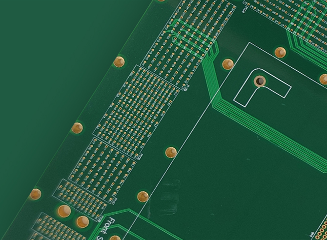
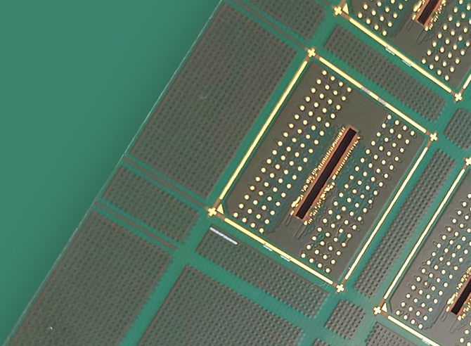
Due to the increasing popularity of electronic devices, such as smartphones and tablets, JOVEPCB Enterprise Ltd. has been continuously investing in the development of new technology to improve the performance and capability of its products. This includes the establishment of a new plant that will allow the company to produce more advanced PCBs, such as Substrate-like-PCB&MEMS(Micro Electrical Mechanical System)PCBs.
JOVEPCB Enterprise Ltd. is a manufacturer of anylayer and substrate-like-PCBs, which are ideal for various consumer electronic devices such as smartphones and tablets. These types of PCBs are also suitable for the industrial control and automotive industries. We can offer substrate-like PCB solutions that meet the low-loss, high-speed needs for high-reliability applications.

What can we do?
Technical Characteristics
|
|

Manufacturing Process

Technical Parameter
| No. | Capabilities | Standard Production | Advanced Production | ||
|---|---|---|---|---|---|
| 1 | Panel size | Double sided | ENIG/ENEPIG | 410mm*510mm | 410mm*510mm |
| ≥4 layers | ENIG/ENEPIG | 410mm*510mm | 410mm*510mm | ||
| 2 | Stack up | Min Dielectric ThK | 6um(ECM) | 3um(ECM) | |
| Max Layer count | 8L | 12L | |||
| Final board ThK Tolerance | ThK≤1.0mm | ±30um | ±20um | ||
| ThK>1.0mm | ±50um | ±30um | |||
| 3 | Line/Space | Inner Layer | 1/3OZ | 45um/45um | 35um/35um |
| 1/2OZ | 55um/55um | 45um/45um | |||
| 1OZ | 65um/65um | 55um/55um | |||
| Outer layer | 1/3OZ | 45um/45um | 35um/35um | ||
| 1/2OZ | 55um/55um | 45um/45um | |||
| 1OZ | 65um/65um | 55um/55um | |||
| Pad Tolerance | ≤100um | ±30um | ±20um | ||
| >100um | ±40um | ±30um | |||
| 4 | Drill | Mechanical Drill size | 0.1-4.0mm | 0.1-4.0mm | |
| PTH Hole Tolerance | ±50um | ±50um | |||
| NPTH Hole Tolerance | ±30um | ±25um | |||
| Plated slot tolderance | Long slot | ±75um | ±50mm | ||
| Short Slot | ±100um | ±75um | |||
| 5 | Min BGA | Min BGA/ BGA pitch | 400um | 350um | |
| 6 | Laser | Laser hole size | 75um | 50um | |
| Min. distance from laser hole to laser hole | 150um | 110um | |||
| Laser hole size | ≤0.8:1 | ≤1:1 | |||
| Min. annual ring | 50um | 35um | |||
| 7 | Embedded Capacitance Tolerance | 3M | C1012 | ±20% | ±20% |
| C2006 | ±20% | ±20% | |||
| C4003 | ±20% | ±20% | |||
| 8 | Resistor Conductor Tolerance |
Omega | 25Ohm/□ | ±20% | ±20% |
| 40Ohm/□ | ±20% | ±20% | |||

Products & Technologies

Contact Us and Support
Keep an eye on us and keep abreast of the latest product
information and trends.
Technology
Copyright © Copyright @ JOVEPCB Enterprise Ltd. | Guangdong ICP Filing No. 18041806


