Technology
High-Density Interconnect (HDI) PCBs

Your reliable PCB solutions provider
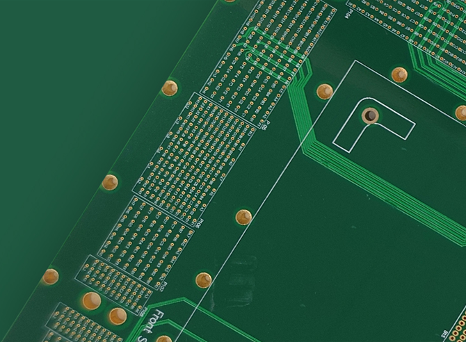
High-density PCBs are commonly used to connect various components in small packages. They are equipped with fine feature technology to improve their electrical performance. This type of board has a smaller footprint and is ideal for reducing the size of the components. In addition to reducing the size of the PCBs, these features also improve the performance of the electrical components.
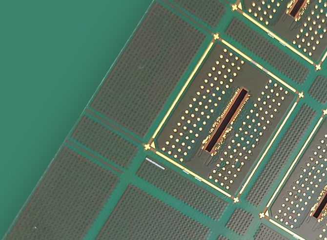
HDI PCBs are used in the design of advanced technology products, such as high-speed chips and large pin-count and fine pitch components. Due to their various features, such as fine lines, laser microvias, multiple laminations and high speed laminates, these PCBs offer a wide range of functions per unit area. With the addition of stacked microvias, these PCBs provide the necessary signal integrity and routing solutions for today's demanding applications.
High-density PCBs (HDI PCBs) are designed with the latest technologies to improve their functionality and signal integrity. These features allow them to utilize the same or less area for multiple features. The rapid emergence and evolution of new technology in the printed circuit board (PCB) industry has allowed companies to create new products that are designed to meet the needs of today's society. Some of these include 5G communications, wearable medical devices, and autonomous vehicles.

What can we do?
Since the introduction of high-density interconnect (HDI) printed circuit boards, their use has been increasing in the electronics industry. This is due to the introduction of new components such as BGA and CSP. JOVEPCB Enterprise Ltd. offers a wide range of technologies, including from 1+N+1 HDI , up to any layer HDI(ELIC).
Technical Characteristics
|
|

Manufacturing Process

Technical Parameter
| No. | Capabilities | Standard Production | Advanced Production | ||
|---|---|---|---|---|---|
| 1 | Stack up | Blind/Buried/Anylayer board | Lamination times | MAX≤5times | MAX≤6times |
| Copper thickness | Inner layer | 1/3OZ-2oz MAX 2OZ |
1/4OZ-2oz MAX OZ |
||
| Outer layer | 1/3OZ-3OZ | 1/3OZ-2OZ | |||
| Min Dielectric ThK | 35um(1027) | 30um (1017) | |||
| Structure | 1-N-1 / 2-N-2 / 3-N-3 | 1-N-1 / 2-N-2 / 3-N-3 / 4-N-4 / ELIC(12L) | |||
| Layer count | 4-24 | 4-34 | |||
| 2 | Min. Line/Space | Min L/W (inner) | 2/2mil (50/50um) | 1.6/1.6 mil ( 40/40um) | |
| Min. L/W (Outer) | 2.4/2.4mil (60/60um) | 2/2mil (50/50um) | |||
| 3 | Line/Space | Inner Layer | Tenting | 2/2mil (50/50um) | 1.6/1.6 mil ( 40/40um) |
| mSAP | 1.4/1.4mil (40/40um) | 1.2/1.2mil (35/35um) | |||
| Outer layer | Tenting | 3/3mil (75/75um) | 2.4/2.4 mil ( 60/60um) | ||
| mSAP | 2.4/2.4mil (60/60um) | 2/2mil (50/50um) | |||
| Pad size | inner layer min size | 225um | 200um | ||
| outter layer min size | 225um | 200um | |||
| 4 | Drill | min Mechanical Drill size | 0.2mm | 0.15mm | |
| PTH plating A/R | ≤8:1 | ≤10:1 | |||
| PTH Hole Tolerance | ±0.075mm | ±0.075mm | |||
| NPTH Hole Tolerance | ±0.05mm | ±0.05mm | |||
| Plated slot tolerance | Long slot | ±0.075mm | ±0.075mm | ||
| Short Slot | ±0.1mm | ±0.1mm | |||
| 5 | Min BGA | Min BGA/ BGA pitch | 0.4 | 0.35 | |
| 6 | Laser | Min. Laser hole size | 75um | 50um | |
| Min. distance from laser hole to laser hole | 0.025mm | 0.025mm | |||
| Laser hole plating A/R | ≤0.8:1 | ≤1:1 | |||
| 7 | Soldermask | Color | Green,Yellow,Black,Blue,Red, White, Matt green | Green,Yellow,Black,Blue,Red, White, Matt green | |
| SM ThK | Single print thickness | 10-30um | 10-30um | ||
| Min SM dam | 3.0mil | 2.5mil | |||
| 8 | Impedance | Capability of Impedance | Single line impedance<50Ω | ±3.5Ω | ±3.5Ω |
| Single line impedance≥50Ω | ±10% | ±7% | |||
| Differential line impedance | ±10% | ±7% | |||
| 9 | Tolerance capability | Patten size tolerance | pad size tolerance | ±20% | ±15% |
| line tolerance | ±20% | ±15% | |||
| patten to outline | +/- 0.0075mm | +/- 0.0050mm | |||
| Registration tolerance | laser A/R | 100um | 75um | ||
| PTH A/R | 100um | 75um | |||

Products & Technologies

Contact Us and Support
Keep an eye on us and keep abreast of the latest product
information and trends.
Technology
Copyright © Copyright @ JOVEPCB Enterprise Ltd. | Guangdong ICP Filing No. 18041806


